


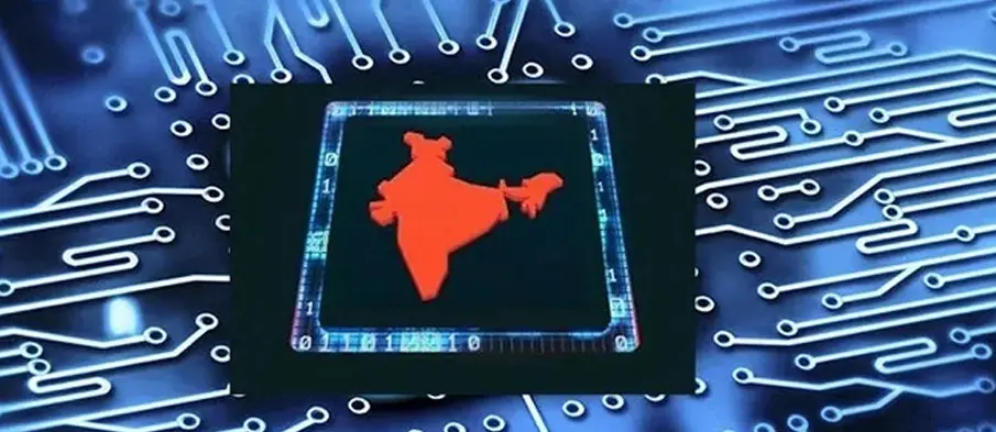
India is set to develop its own Intellectual Property across six key semiconductor systems under the India Semiconductor Mission, Union Minister for Electronics and Information Technology Ashwini Vaishnaw said while outlining the progress of the country’s national chip strategy.
Addressing the media, the Minister stated that India is steadily advancing toward becoming one of the most significant semiconductor nations globally by 2035. He noted that the focus will be on building indigenous IP in compute, RF, networking, power, sensor, and memory technologies.
Sharing milestones achieved since the launch of the mission, Vaishnaw said, “On the completion of four years of India semiconductor mission, 10 projects are under construction, production for four projects will start this year and 24 project startups have designed semiconductor chips, and in 315 educational insitutions students have received training to design semiconductor chips…We will create India’s own IP in 6 systems of compute, RF, networking, power, sensor and memory through India Semiconductor Mission…As we go into 2029, India will become a major player in the semiconductor industry…By 2035, India will be among the most important semiconductor nations in the world…”
Earlier in the day, the Minister interacted with representatives from 23 semiconductor design companies approved under the Design Linked Incentive (DLI) Scheme of the Semicon India Programme. During the interaction, he said that India’s semiconductor design ecosystem has reached a stage where companies are moving beyond conceptual plans to delivering functional chip solutions.
Vaishnaw highlighted that access to Electronic Design Automation tools was a key challenge at the start of the programme. He pointed out that the provision of free, sovereign access to EDA tools through C-DAC has given Indian designers a significant advantage in the global design landscape. “When we started this program, a major concern was access to EDA tools and access to IP,” he said.
He also emphasised that financial backing becomes easier once startups demonstrate working products, adding, “Funding becomes much easier once you have developed a working project; otherwise, it’s just a PPT presentation.”
The Minister concluded that the progress achieved so far has laid a strong foundation for India’s semiconductor ambitions, positioning the country to play a much larger role in the global chip ecosystem over the next decade.


