


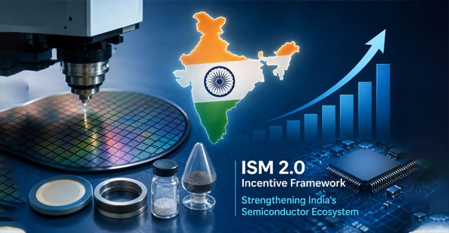
India Semiconductor Mission 2.0 (ISM 2.0) is expected to introduce a 30% capital subsidy for companies manufacturing semiconductor equipment and materials, along with a five-year production-linked incentive linked to domestic value addition.
The proposed production-linked incentive would start at 10% of the domestic bill-of-materials value in the first year, before declining to 8%, 6%, 4%, and 2% over the following four years. Combined government support would be capped at 50% of eligible capital expenditure.
Detailed guidelines are expected shortly, meaning the reported incentive structure remains provisional until it is formally notified.
Support to Extend Beyond Semiconductor Fabrication
The framework is intended to expand public support beyond semiconductor fabrication and packaging into the supporting industrial base.
Expected eligible activities include semiconductor-grade materials, equipment manufacturing and assembly, research and development facilities, and test and characterisation infrastructure.
These areas cover parts of the value chain where Indian projects continue to depend on imported machinery, chemicals, gases, precision components, and specialist testing capabilities.
Semicon 2.0 Approved With ₹1,27,500 Crore Budget
The Union Cabinet approved Semicon 2.0 in July with a budget of ₹1,27,500 crore.
The mission has six stated pillars:
- Chip and system design
- Semiconductor machines and materials
- Additional fabrication plants
- Expansion of assembly, testing, marking and packaging capacity
- Research and development
- Talent creation
The government has said that India’s first wafer fabrication plant under the programme is scheduled to be commissioned in 2028. Future support will cover silicon, compound-semiconductor, discrete-component, and display fabrication facilities.
Second Phase Builds on 12 Manufacturing Projects
ISM 2.0 builds on 12 manufacturing projects approved under the first semiconductor mission, representing cumulative investment of more than ₹1.64 lakh crore.
These projects include one silicon fabrication plant, a silicon-carbide facility, an integrated gallium-nitride micro-LED display fab, and nine packaging units.
Micron, Kaynes, and CG Semi have begun commercial production, while another approved project is expected to commence production during 2026.
Chip-Design Projects and Training Also Expand
On the design side, 24 projects involving startups and small businesses have received financial support.
Another 105 companies have been granted access to electronic-design-automation tools for developing chips and systems used in satellite communications, drones, surveillance, IoT devices, AI systems, telecom equipment, and smart meters.
The government also says that 315 universities are using advanced chip-design tools, while approximately 68,000 students have been trained.
Final Rules Will Determine Implementation
The emerging incentive design combines capital support with production-linked payments intended to encourage domestic sourcing and value addition.
Implementation will depend on the final definitions of eligible equipment, qualifying domestic bill-of-materials expenditure, project milestones, and the process for coordinating central support with state-level incentives.



 is expected to introduce a 30% capital subsidy for companies manufacturing semiconductor equipment..)