

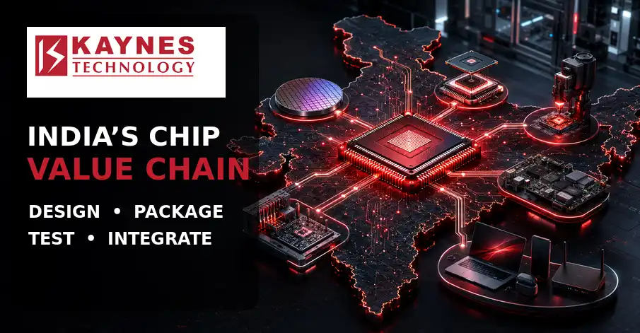
Kaynes Semicon is preparing a broader push into the semiconductor value chain, with plans to explore wafer fabrication, compound semiconductors, advanced packaging, and materials and equipment manufacturing through global technology partnerships and joint ventures.
Chief executive Raghu Panicker has said the company is in advanced discussions with international technology companies for these areas. The expansion plan is expected to be routed through applications under the next phase of the India Semiconductor Mission, subject to the government opening the application window. The company is looking to submit project proposals by mid-August.
The move marks a significant broadening of Kaynes Semicon’s ambitions beyond assembly and packaging. Rather than attempting to build all capabilities independently, the company is looking at a partnership-led model, a structure that could help it access process know-how, equipment capability, manufacturing methods, and customer linkages faster than a purely organic buildout.
India’s semiconductor programme has so far focused on creating domestic capacity across multiple layers of the chip stack, from outsourced semiconductor assembly and test operations to fabrication, display manufacturing, compound semiconductors, and design-linked incentives. Kaynes Semicon’s proposed expansion fits into that broader policy direction, where domestic firms are being encouraged to move from isolated manufacturing nodes toward more integrated electronics and semiconductor ecosystems.
The timing is important because demand for chips tied to artificial intelligence, telecom, automotive electronics, industrial systems, and defence electronics continues to rise. For Indian semiconductor players, the next phase of competitiveness will depend not only on approved incentives but also on whether they can bring credible technology partners, anchor customers, and execution discipline into capital-intensive projects.
Kaynes Semicon’s approach also reflects the practical constraints of semiconductor manufacturing. Wafer fabrication and advanced materials require large capital commitments, deep process expertise, cleanroom infrastructure, supply-chain maturity, and long qualification cycles with customers. Joint ventures and technology partnerships can reduce some execution risk, but they also make partner selection, governance, technology transfer terms, and project sequencing central to the outcome.
If the company proceeds with applications under the next phase of the India Semiconductor Mission, the proposals will be watched as a test of how Indian electronics manufacturers are positioning themselves for a deeper role in chip manufacturing. The development also places Kaynes among the domestic companies trying to convert India’s semiconductor policy push into operational manufacturing capacity rather than remaining limited to downstream electronics assembly.